


NT-MDT in the USA. News Letter #3, January 2015
28.01.2015
 Printable version Printable version |
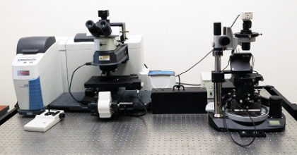 AFM/Raman instrument based on NTEGRA Spectra (NT-MDT) scanning probe microscope and Thermo Scientific™ DXR™ Raman microscope. |
|
| Combining AFM with Raman: NT-MDT and Thermo Fisher Scientific | ||
| Since last year the joint efforts of NT-MDT and Thermo Fisher Scientific, one of the main manufacturers of scientific instrumentation in the world, have led to the development of the combined AFM/Raman instrument (see the photo above) capable of simultaneous recording of AFM images and Raman maps at specific wavebands, including tip-enhanced Raman spectroscopy experiments. The capabilities of this instrument were verified in a number of studies of various materials | and the collected data were presented in the Application Note: “Characterization of Materials with a Combined AFM/Raman Microscope” and were reported in the latest NT-MDT Webinar on January 12. Currently, there is a series of coordinated engineering, application, marketing and sales efforts from both companies for the successful promotion of the instrument in the USA and worldwide. | |
| Quantitative Nanomechanics with HybriD™ Mode | |||||
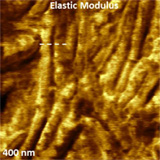
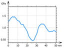
| Local nanomechanical studies are an essential capability of AFM, which can be realized in contact mode and oscillatory resonant and non-resonant modes. The elastic modulus and work of adhesion can be extracted from the force curves. It is done most efficiently in the HybriD mode where the quantitative maps of these properties can be obtained on-line simultaneously with the height images. The validity of the quantitative measurements is verified on the test set of neat polymer samples (polystyrene and two different polyethylenes) with macroscopic Young modulus in the range from tens of MPa to several GPa. We are exploring this functionality in depth, and in case of heterogeneous samples we have achieved the mapping of the elastic modulus at the sub-100 nm scale. The illustration of the high-resolution modulus mapping is given by the elastic modulus map (512´512) of high-density polyethylene (HDPE), see below. In this picture an amorphous interlamellar layer of 10 nm in width is clearly seen in the map and in the related cross-section. |
More examples of high-resolution mapping of mechanical properties of polymers will be shown in the upcoming NT-MDT Webinar on February 12. The analysis of these curves in terms of solid state deformation models is complicated due to a non-trivial relation between amplitude/phase and the tip-sample forces. The problem can be solved as shown in our research paper “Modeling and Measurements in Atomic Force Microscopy Resonance Modes” by S. Belikov et al, which is accepted for publication at American Control Conference, 2015. The experimental verification of these calculations is on the way. |
||||
|
|||||
| From the Laboratories | ||||||||||||
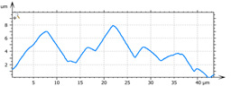
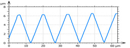
| In Tempe office, we appreciate greatly the requests of the researchers regarding different capabilities of our AFM microscopes, and we are happy to help them by evaluating their samples. In one of such interactions with Salman Manzoor (Holman Lab, ASU) we have been challenged by an examination of Si profiles of several microns in height. Such profiles are essential features of black Si – the light- harvesting element of solar panels. We have performed these measurements with Titanium scanning probe microscope using the high-aspect ratio |
probes with single crystal diamond tips. Two examples of these studies are given below. The first height image shows the Si pyramids, and the inverted pyramids are shown in the second 3D height image. The cross-section profiles reveal the height corrugations in the 6-8 microns range. The precise evaluation of the sample topography of these black Si samples and its correlation with light trapping is important for improving the solar cell efficiency. | |||||||||||
|
||||||||||||
| Forthcoming NT-MDT Events: 2015 | ||
|
February 12: Webinar “High-Resolution and Quantitative Mapping of Mechanical Properties”, which is based on studies of elastic modulus and work of adhesion of polymers in the HybriD mode. February 19-20: NT-MDT AFM/Raman Workshop at Carnegie Mellon University (Pittsburgh, PA), which includes technical presentations and demonstration sessions using NT-MDT microscopes. |