


NEXT Scanning Probe Microscope: Visualization of Surface Nanostructures and of Morpholog
Application Note 086 (pdf 3.6 Mb)
Sergei Magonov, NT-MDT Development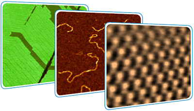
Achieving molecular-resolution in the intermittent contact mode
Enhancement of surface visualization with a force control
Metrological aspects of profiling of rough surfaces
Visualization of surface structures with unique resolution is the main function of A tomic Force Microscopy and the practical realization of surface profiling with the in termittent contact mode has r ecently advanced to the molecul ar-scale level. This is the important AFM feature yet the value of the technique is much broader and it includes its ability to reveal ac onformation of single macromolecules, the sub-surface structures of soft materials, ac omplexity of porous morphology of industrial membranes and clarify the defects of semic onductor crystals. The different aspects of the visualization of surface structures, which include an op timization of the tip force and shape, most efficient experimental routines and image analysis, are considered in this appli cation note.
INTRODUCTION
Microscopic observations were revolutionized with the development of Scanning Tunneling Microscopy (STM) [1] and Atomic Force Microscopy (AFM) [2] – proximal probe methods that provide visualization of surface structures down to the atomic scale. For over 20 years these complimentary techniques were intensively applied by researchers, with AFM being in the leading position due to its applicability to a broader range of materials.
Unfortunately, the capabilities of examination of atomic and molecular structures with AFM, particularly with amplitude modulation (AM) mode, are inferior compared to STM.
Recently, with advances in instrumentation this difference is shrinking. One of the substantial factors influencing the image resolution is the sensitivity of the optical lever detection scheme applied in AFM microscope.
The signal-to-noise level of the optical detection in NEXT has been improved to < 20 fm/√Hz level. In addition, the noise of the high voltage amplifier has been lowered and a soft approach procedure, which prevents a breakage or blunting of a sharp tip during engagement, was implemented. The combined improvements from these features were essential for recording the images presented below.
GENERAL ISSUES AND MOLECULAR-SCALE IMAGING
Before presenting the analysis of the experimental AFM images obtained on different materials it is important to introduce some basic features of AM mode, which was exclusively applied for our studies. The imaging modes in AFM can be classified by the type of probe-sample interaction parameter, which is sensitive to the tip-sample forces and which is employed in the feedback loop during the scanning the sample surface. The probe deflection is directly proportional to the tip-sample force. The cantilever deflection is used in the contact mode and in one of the oscillatory modes, which is realized at a frequency that is far below the probe’s flexural resonance.
The amplitude and frequency of the probe, which are influenced by the tip-sample forces, are used for a feedback in AM and frequency modulation (FM) modes. In these complementary modes, the imaging is performed at or close to the probe resonant frequency. Due to operation at the resonant frequency these modes offer a superior control over the tip-sample forces. The probe oscillatory motion and interaction with a surface profile can be described by the Euler-Bernoulli equation.
The asymptotic solution of this problem for a particular type of tip-sample force interactions is obtained as a set of two equations with four variables: the probe frequency, amplitude, phase and surface profile [3]. In AM (FM) mode frequency (phase) and amplitude (frequency) are fixed, and the experimental images of the surface profile and the probe phase (frequency) can be simulated as the solutions of these equations. For the case of conservative force interactions, the equations are simpler and can be utilized for modeling of AFM images.
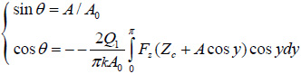
Here, k – spring constant of the probe, Q1 – quality factor of the probe, Ѳ - phase of the probe, Zc – surface profile; A and A0 – set-point amplitude and amplitude of the probe before it comes into tip-sample interactions; Fz – force the originated from mechanical and electromagnetic tip-sample interactions.
AM is the most common imaging mode and it can be applied in different regimes from the non-contact to intermittent contact operations through probing the attractive and repulsive force interactions with a sample. When the set-point amplitude is close to the amplitude of a non-interacting probe then the tip-forces are small which is favorable for gentle surface imaging.
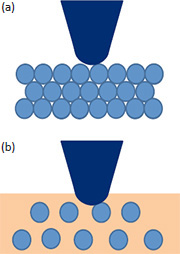
The forces can also be reduced when the oscillation amplitudes are lowered to the nanometer or even sub-nanometer range, but the actual environment causes some restrictions to the range of the applicable amplitude. In low-force operation the tip-sample contact area is also small just a fraction of the apex diameter. Therefore, such operation will be favorable for high-resolution imaging. This is only true when the structures of interest are at the topmost surface, Figure 1a. With some polymers the top surface might be enriched in featureless amorphous material having low surface energy and the structures of interest are hidden underneath this layer, Figure 1b. In such cases the tip penetration at lower Asp/A0 ratio is required for visualization of these structures. The influence of the tip size and the tip-sample force interactions on the AFM image of the surface objects is demonstrated in Figures 2a-c. The AM images of a model array, which is made of individual spheres with different elastic modulus and various spacing, were obtained with the computer simulator, Figure 2a.
The true reproduction of the array structures was achieved only in the low-force imaging with the atomically sharp probe. When the tip-size increases the spheres appear larger yet the spacing in the bottom row, where the spheres are closely packed, remains practically the same, Figure 2b. This explains how high-resolution lattice imaging can be achieved in imaging with typical Si probe whose tip has an apex with 5-10 nanometer radius. When the tip-sample force is elevated, the softer spheres are more depressed and they are seen closer to their true size, Figure 2c. The demonstrated trends in AM imaging of soft materials such as polymers and biological specimens should be considered in the analysis of image data.
ATOMIC-AND MOLECULAR-SCALE IMAGING
High-resolution AM and FM images of the atomic- and molecular scale are typically obtained on crystallographic lattices and aligned layers of macromolecules. Although the imaging of such structures even with the visualization of single defect [4] should not be strictly considered as a proof of true atomic resolution, it is an indicator of a higher performance microscope. Several examples of high-resolution imaging with NEXT microscope are presented in Figures 3 and 4.
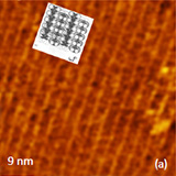
Crystalline lattices of highly oriented pyrolitic graphite (HOPG) and mica are represented in the atomic-scale images recorded with scanning tunneling microscope and atomic force microscope operated in the contact mode. Such images obtained with NEXT microscope are shown in Figures 3a-b where the image patterns reproduce the symmetry of the basal planes of these crystals with 0.25 and 0.52 nm periodicities.
The described above instrumental improvements in this microscope also allows recording of the lattices images of calcite crystals while operating in AM mode under water, Figures 3c-d. These images were obtained with regular Si probes and operating amplitudes round 1 nm. The image patterns are consistent with the rectangular lattice of calcite having repeat distances of 0.83 nm and 0.51 nm. The molecular-scale images of organic crystals of tetrathiafulvalene (TTF) -tetracyanoquinodimethane (TCNQ) salt and oriented polytetrafluoroethylene (PTFE), which were obtained in AM mode in air, are presented in Figures 4a-b. The top surface of the salt crystal is the crystallographic ab plane, and it is formed of alternative stacks of TTF and TCNQ running along the b axis.
These stacks are clear seen in AFM height image and the observed periodical image pattern is consistent with the main repeat distances of 1.23 nm and 0.38 nm, respectively, in the perpendicular a and b directions. An ultrathin layer of polytetrafluoroethylene (PTFE) that is deposited on a glass substrate by rubbing at high temperature is the useful sample for imaging of single chains. The close packed polymer chains, which are aligned along the rub-bing direction, are seen in Figure 4b.
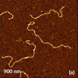
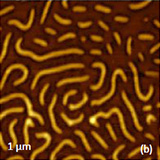
The inter-chain spacing in this arrangement is close to 0.56 nm that was found in TEM micrographs of virgin PTFE [9]. Visualization of the closely-packed PTFE molecules was first demonstrated in contact mode [10] and now it can be routinely achieved in AM mode. Although the images of surface periodical structures down to the atomic-level are often outlined as the STM and AFM highlights, the unique features of this instrument is the visualization of single biological and synthetic macromolecules on different substrates. The examples of AFM images showing strands of DNA and poly(butyl acrylate) brush molecules, both placed on mica, are presented in Figures 5a-5b. The polymer macromolecules have large number of side chains and, therefore, the chains have an expanded shape. Having in mind the tip-size and tip-force effects, the most accurate chain parameters will be their contour length and conformation. The contour length of the macromolecules is related to the molecular weight and this information compliments the chromatography data. AFM visualization of macromolecules branching, star-like shapes and other conformations is highly valued by synthetic chemists creating new materials.
EXPLORING SURFACE ORGANIZATION OF NORMAL ALKANES
Molecular ordering of relatively simple molecules of normal alkanes on different substrates has attracted the researchers’ attention from different viewpoints. First of all, these chain molecules exhibit an epitaxy ordering on layered materials (graphite, MoS2, etc.), and studies of alkane/graphite interfaces is relevant for understanding the similar effects in composites of polyolefin and graphite flakes.
Another phenomenon, which is known for alkanes and their derivatives, is surface freezing in which the interfacial layers (at liquid-air or liquid-substrate interfaces) solidify at a temperature where the bulk material is still liquid. The adsorbates of alkane on graphite were also among the first organic materials whose organization was visualized with STM in the experiments conducted in droplets of saturated alkane solutions deposited on the substrate.
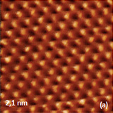
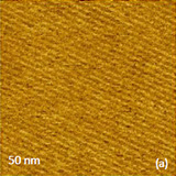
When thin layers of normal alkanes CnH2n+2 are deposited on graphite and inorganic layered substrates (MoS2, MoSe2, WS2, WSe2, etc.) in their AFM image one can distinguish linear features separated by dark borders, which represent the alkane lamellae.
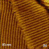
The latter are two-dimensional arrays, which are formed of closely packed chain molecules flat-lying on these atomically-smooth substrates. In many cases the lamellae width corresponds to the length of alkane chain as it seen from the images of C18H38 and C36H74 adsorbates on graphite in Figures 6a-b. The spacing in the patterns are close to the expected length of the molecules: 2.8 nm (C18H36) and 4.5 nm (C36H74).
In case of the C36H74 adsorbate the alkane lamellae cover the graphite grains with different orientation.
There are some claims that a match of the repeat distance along the alkane chain in the zigzag conformation (0.25 nm) with one of the graphite spacing insures the molecules epitaxy. However, the flat-lying lamellae of normal alkanes are also observed on the layered substrates whose lattice differs from the graphite one. As the alkane molecules become longer they can be considered as a model of polyethylene and the ultra-long alkane C390H782 possess a number of features
similar to the polymer.
When the ultra-long alkanes are deposited on graphite their lamellae are identified by the increased width and some other features. The bright wavy strands with a width close to the length of C122H246 (14 nm), C242H486 (27 nm) and C390H782 (49.7 nm) molecules are resolved in the images of these alkanes in Figures 7-8.
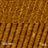
These strands represent the alkane lamellae, and this assignment is supported by the finding that the steps between the layers and in the depressions are multiple of 0.5 nm, that is the size of single alkane chain. First, we consider the nature of the contrast in AFM images of alkanes (Figure 7a-b), and then will comment on the shape of the lamella. The origin of the image contrast, which helps identifying the alkane lamellae, can be understood from the study of the C122H246
alkane at different tip-sample forces, Figure 7c.
At the low force (a top part of the image) one can see slightly elevated linear features with spacing close to the lamellar width.
As the tip-force increased the image pattern has changed and the elevated location transformed into depressions. This change is reversible and, most likely, reflects the tip interactions with the molecular groups at the lamellae edge. The border between the lamellae is populated with the end – CH3 groups of the alkane chains.
These groups are slightly bigger than the –CH2– groups forming the chains and, therefore, should be elevated with the respect of flat-lying lamellae. From the other hand, the – CH3 end groups are less fixed and their mobility means that the probe might displace them and this will lead to a small depression seen at the elevated force imaging. It is worth noting that in many cases the control of the low-force regime might be difficult and the images with the depressed lamellae
borders are recorded more frequently.
The wavy shape of the lamellae in C122H246 and C242H486 alkanes, Figures 6a, is rarely observed in the adsorbates of smaller alkanes. A close packing of the chains inside lamellae need to find a compromise in accommodating the bulky end groups. This can be realized by a slight relative displacement of the neighboring chains that leads to a slightly curved shape of lamellar ribbons of C122H246 and C242H486. In case of C390H782
alkanes, whose adsorbates exhibit the parquet-like morphology (Figure 8b), this effect is much stronger and synchronized.
As a result the alkane chains become tilted within lamellae at the angle ~30 degrees with respect to the orthogonal direction to the lamellae border. The tilt leads also to the reduction of the lamellar width.
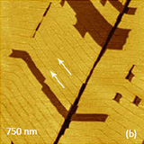
This observation is consisted with the earlier results, which also show that on heating the parquet-like morphology transferred to the stripped morphology, in which the molecular tilt is eliminated, and the lamellar width become equal to the length of the extended chain [14]. One more structural defect, which is pointed by white arrows, is observed in the image of C390H782 alkane, Figure 6b.
This linear dislocation is characterized by a shift of neighboring lamellae for a half of the spacing, Figure 8d. So far, we have described the molecular ordering of adsorbates in thin top layers of alkanes, which are easily accessed by the AFM probe. It is also quite important to examine the material organization in the layer that was in a direct contact with the substrate. The related samples of alkanes and polymers can be prepared by stripping them from the graphite after the material underwent epitaxial
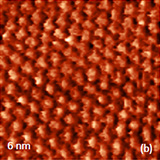
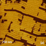
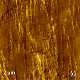
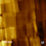
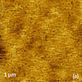
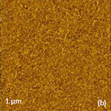
crystallization. The images of epitaxial morphology and lamellar structure of C36H74 alkane which was epitaxially crystallized on graphite are shown in Figures 9a-d.
Multiple crystalline blocks, most of a rectangular habit, are distinguished in the large-scale images. One of the blocks has been examined at the smaller scale and imaging at the elevated forces revealed straight lamellae of 4.5 nm in width that were covered by a thin disordered alkane layer, Figure 9d. Epitaxial ordering of polyethylene and other polymer on different substrates is the know research area and AFM contributing to the related studies for a long time. We will illustrate such
applications with the images of high-density polyethylene (HDPE), Figure 10a-b.
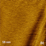
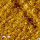
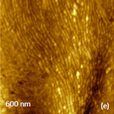
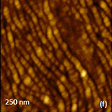
The surface of the polymer, which was in contact with graphite during crystallization from melt, is characterized by extended strands of 50‑80 nm in width. A few of these strands are shown in the high-resolution image in Figure 8b. The extended polymer chains, which might reach ~50 nm in length, are presumably oriented along the short direction of the strands. This sample is the proper object for high-resolution imaging with intent of visualizing the polymer chains.
MORPHOLOGY AND LAMELLAR STRUCTURE OF SEMI-CRYSTALLINE POLYMERS
AFM studies of semicrystalline polymers in different samples have been performed for a long time. A common feature of semicrystalline polymers is a presence of amorphous and crystalline phases. The amorphous phase is generally a featureless material and it is characterized by glass transition temperature, at which it undergoes the transition from rubbery to glassy state accompanied by a drastic change of elastic modulus.
The crystalline part of the polymers is denser than the amorphous and it is represented by lamellar structures formed by the folded chains. Typically, the lamellae are formed as extended sheets with thickness in the 5-40 nm range. Due to variety of reasons (confined geometry, extensive chain branching, a lack of material, etc.) the lamellae can be reduced to the fibers and even grains – the structures that preserve the folded chain core and less ordered exterior.
At the micron scale, these structures are assembled into spherulitic objects of different completion. The essential features of AFM imaging of semicrystalline polymers are demonstrated in Figures 11-12.
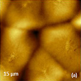
First is taken from studies of a blend of two polyethylenes that has relatively poor crystalline content. Surface morphology of the blend is characterized by spherulites, whose slightly deformed shapes reflect their growth restricted by the neighbors. For polyethylenes the glass transition temperature of amorphous phase is well below room temperature, therefore, at ambient conditions these materials are mechanically heterogeneous due to difference of elastic modulus of amorphous and crystalline components.
This circumstance facilitates the detection of the constituents of the semicrystalline polymers.
The images of the part of the spherulite, which were performed at low tip-forces, reveal corrugated surface with few curved features best seen in the phase image. As the tip-force increased, the contrast of the images became more pronounced and the curved structures because well distinguished: brighter than surrounding in the height image and darker – in the phase image. These structures can be assigned to the lamellar edges or polymer fibrils embedded into softer amorphous material. With the
force increase
the tip depresses the amorphous material and, therefore, the stiffer structures become elevated. The phase contrast is also very sensitive to local mechanical properties, and according to the convention chosen for a phase adjustment at the beginning of AFM imaging the darker phase contrast is related to higher local stiffness. It is worth noting that the demonstrated image changes are reversible because the amorphous material being in the rubbery state recovers to its original shape when the load is reduced.
In AFM studies of semicrystalline polymers [i.e. syndiotactic polystyrene, poly(ethylene terephthalate)], and others) whose amorphous phase has glass transition at elevated temperatures, visualization of the crystalline structures requires the imaging at temperatures exceeding the glass transition.
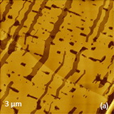
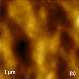
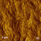
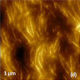
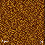
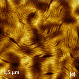
The crystallization conditions essentially influence morphology and nanostructure of semicrystalline polymers as seen from the imaging of poly(vinyledene fluoride) - PVDF samples, which were crystallized from melt in air and in contact with graphite. The air-crystallized polymer formed large spherulites with a depression in its center, Figure 12.
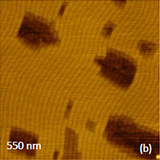
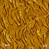
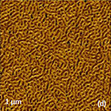
The beams radially emerging from the spherulite center have a complex composition, which includes small lamellar platelets, fibrils and grains, Figure 12b. At higher magnification, the phase image in Figure 12c shows tiny 10 nm thin fibrils. The surface morphology and nanostructure of PVDF sample crystallized in contact with graphite is quite different, Figures 11d-f. At the large scale the relatively flat sheaf-like patterns represent the top surface, Figure 11d. These sheaf-like structures are formed on
arrays of fibrils, which are 10-15 nm wide, Figure 11e. The fibrils, which exhibit grain sub-structure (Figure 11f), are rigid due to high crystallinity content of this polymer.
NANOSCALE ORGANIZATION OF BLOCK COPOLYMERS
Block copolymers are macromolecules, which are composed of two or more chemically different and covalently bonded polymer chains. These chains are typically immiscible, and this leads to the phase separation of block copolymer materials into morphologies of different symmetry. Such phase-separated morphologies have characteristic dimensions in the range from several to tens of nanometers, and therefore, among different applications the block copolymer materials are suggested for nanoscale templates.
AFM has
been often applied to studies of block copolymers with a primary goal of visualization and quantitative analysis of their morphology. It is important to describe how the structural features can be retrieved from the AFM images and how to optimize the visualization of the microphase separation patterns. The image features are typically assigned to structures either according to their particular shapes or dimensions. The contrast can also originate from differences of local mechanical and electric properties of
individual blocks. The triblock copolymer poly(styrene)-b-poly(butadiene)-b-poly(styrene) - SBS is an appropriate sample to illustrate the specifics of AFM imaging of these materials. At room temperature polystyrene blocks are glassy with elastic modulus of 2-3 GPa and the poly(butadiene) blocks are rubbery with elastic modulus of ~16 MPa.
In addition, poly(butadiene) blocks have lower surface energy and wet the surface of the SBS sample. When the SBS film is examined in AM mode the height and phase images depend drastically on stiffness of the applied probe and operation amplitudes: Asp and A0. When Asp is close to A0, the height image presents a relatively smooth topography of this sample and the phase image is practically features-less, Figures 13a-b. With the decrease of Asp
the tip-sample interactions are enhanced and the phase separation pattern appears in the height and phase images, Figures 13c-d. These force-dependent changes are reversible, and they reflect a penetration of AFM tip through the top rubbery layer of poly(butadiene) until it reaches sub-surface alternation of poly(butadiene) and poly(styrene) blocks. At elevated forces, the AFM tip might penetrate only few surface layers. When morphology of bulk samples is of interest then the access to their inner morphology
can be opened by the use of cryo ultra-microtomy or etching of surface material by chemicals or plasma. In the general case, a differentiation of blocks having different Tg can be performed by imaging at elevated tip-sample force at temperatures between their Tg.
A selective swelling of one of glassy components with organic vapor can also facilitate its transition to more mobile rubbery-like state and the sample morphology will be revealed in the AFM experiment. The SBS sample described above was obtained by spin-cast of the block copolymer solution on a piece of Si wafer. In this case, the phase separation of poly(styrene) and poly(butadiene) blocks did not progress far because of relatively fast evaporation of the solvent (toluene).
The improvement of the phase separation order, which might be important for a preparation of block copolymer nanoscale templates, can be reached by annealing of this sample at temperatures above the glass transitions of both components of SBS sample and by annealing it in vapor of common solvent such as toluene. Annealing of SBS sample in toluene vapor leads to a more developed morphology that is shown in Figure 14a.
In such cases the surface corrugations are much more pronounced and the micro-phase separated pattern is seen even at low-force imaging because the wetting layer decorates the profile alternations. The height image of another block copolymer poly(styrene)-b-poly(4-vinyl pyridine) shows different micro-phase separation pattern with slightly twisted cylinders, Figure 14b. Here it is important to warn that the interpretation of AFM images of block copolymers is not always straightforward. For example, the stripped pattern might be assigned either to cylinders or to lamellar edges and a dot-like pattern – either to spheres or standing lamella. Therefore, for the correct judgment one might need to rely on the block copolymer volume composition or microscopic data obtained on the cross-sections of the sample.
CORRUGATED SURFACES
Samples with smooth surfaces with corrugations below 100 nm are best suited for AFM measurements. Therefore, different preparation procedures are applied to make sample surfaces flat. They include spin-casting that leads to smooth films, ultra-microtomy and polishing of bulk samples, hot pressing polymers and metals between atomically-flat substrates and others. However, there are a large number of corrugated technological and industrial surfaces which require AFM analysis, and we will consider several related examples. Microporous membranes made of different materials are important technological structures for various applications.
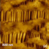
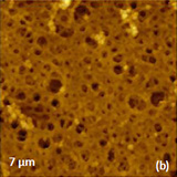
The AFM height images of two polymer membranes are shown in Figure 15. Microporous membrane made of isotactic poly(propylene) – Celgard™ 2400 is characterized by morphology with the alternating fibrillar and lamellar regions that has developed during a combination of mechanical stretching and annealing steps. The voids between the fibrils are used for filtration purposes.
The surface corrugations of this membrane are in the range of tens of nanometers and the extreme caution is needed for gentle profiling of this morphology to avoid the tip-induced perturbations of the fibril orientation and of the size of the inter-fibrillar voids. Surface corrugations of another membrane made of nitrocellulose, which is broadly used for biological and medical purposes, are even larger - in the hundreds of nanometer range, Figure 15b.
With increase of surface corrugations the attention of the AFM practitioners is focused on the probes with tips having high aspect ratio. Unfortunately, the majority of AFM probes are made by etching of crystalline Si wafers that makes crystallographic limitations on the tip shape. Most common Si probes have opening angle around 35 degrees which is not sufficiently sharp to profile the surface corrugations in the micron and above range.
There are a number of specialized probes with the high aspect ratio tips that can be tried for this purpose. The related point is the tip characterization, which can be performed at its best with TEM, yet this possibility is not routine for most of AFM users. In an alternative approach, one can use the test structures with the sharp spikes that can image your tip during scanning of such sample.
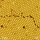
Yet this characterization is most relevant to the tip apex than to the tip profile, and imaging of hard spikes can also make the tip dull. Another possibility of tip characterization might be developed by imaging of close-packed latex spheres.
Actually, AFM studies of polymer latex systems have been useful for monitoring of film formation processes in paints and related systems and provide correlations between the surface roughness of latex-based coatings and their optical properties.
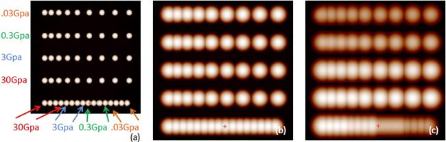
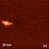
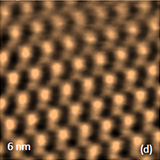
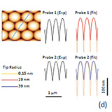
After deposition of latex material from suspensions on flat substrates the individual spheres form ordered multilayer arrays. The image of poly(styrene) latex with spheres of 400 nm in diameter reveals surface locations with a precise hexagonal order, Figure 15c. The surface profile taken along the spheres in the direction indicated with a line (Figure 15d) can be employed for not only qualitative and also quantitative evaluation of the tip profile. This suggestion was verified in the analysis of the experimental
profiles obtained with two different probes: a regular Si probe and conducting Si probe whose tip size was enlarged with an excessive Pt coating.
The ideal surface profiles along the same direction were simulated on a model sample of the close-packed 400 nm hard spheres. It was found that theoretical profiles with tips of radius 19 nm and 39 nm best matched the experimental data as seen in Figure 15d (right) where the profile for an atomically sharp tip is also shown.
SEMICONDUCTOR FILMS
Epitaxially grown films of wide-bandgap semiconductors (e.g. SiGe and ZnO) are widely used for thin film transistors, light emitting diodes and in photovoltaic devices.
The deterioration of crystal perfection influences their band gap and efficiency therefore a comprehensive characterization of crystal defects of an epitaxially grown film in terms of their type, density and spatial distribution is essential for the development of the semiconductor devices.
Therefore, the characterization of defects in epitaxial semiconductor films is the important research field addressed with a combination of diffraction and microscopic methods including AFM. The visualization of local surface defects in AFM images compliments TEM studies and helps in interpreting of averaged structural information collected in the diffraction studies. AFM imaging of semiconductor films, which are much stiffer than the probe, should be performed at low tip-sample forces.
This helps avoiding the tip damage and improving the image resolution by minimizing the tip-sample contact area. Figure 16 presents four height images recorded on the epitaxially-grown films of SiGe on Ge and Si substrates and ZnO on sapphire. The large-scale image in Figure 16a was obtained on SiGe layer on Ge, which is characterized by relative small density of dislocations loops (2.85x102 cm-1) determined with X-ray analysis. Although such samples are characterized by atomically-smooth
surface, few dislocations and cracks, which are shown in this image, can be found in few locations.
The width and length of these imperfections can be defined quite reliable, yet the defect depth analysis is limited by the aspect ratio of the applied probe. The images in Figures 16b-c were obtained on SiGe layers on Si and Ge substrates, which are characterized by high density of the dislocations loops (7.5x104 cm-1 and 2.4x105 cm-1).
Surfaces of these films underwent drastically changes. The corrugated morphology in Figure 16b is formed by arrays of elevated nano-size crystals with a rectangular shape and nearby pits of different size and depth. The pits also have straight corners that reflect their relevance to the crystallographic directions. Another type of corrugated morphology is found in the epitaxial film shown in Figure 16c. Multiple trenches and elevations of this surface are aligned in orthogonal directions of
the crystal lattice.
These AFM finding are pointing out the effects of internal stress generated by dislocations loops on the surface morphology. The image of the epitaxial ZnO film on sapphire in Figure 16d revealed another type of surface defects generated in this sample. This morphology is characterized by a radial symmetry and only traces of the rectangular crystalline lattice were found in the amplitude images.
SUMMARY
This application note presents the results of AFM visualization of different samples performed with the NEXT microscope. The imaging was performed in AM mode at scales from several nanometers to tens of microns and various objects starting with chain macromolecules were recorded in the images.
Several important issues of optimization of AFM experiments on soft and hard surfaces were explained and demonstrated. A choice of probes and means of their characterization were also addressed.
ACKNOWLEDGEMENTS
Prof. G. Ungar (University of Sheffiled, England), Prof. S. Sheiko (UNC Chapel Hill, NC), and Prof. N. Faleev (ASU, Tempe, AZ) are thankful for the samples which were used for this work.
REFERENCES
[1] G. Binnig, H. Rohrer, C. Gerber, and E. Weibel “Surface studies by scanning tunneling microscopy” Phys. Rev. Lett. 1982, 49, 57–61.
[2] G. Binnig, C. F. Quate, and Ch. Gerber “Atomic force microscope” Phys. Rev. Lett. 1986, 56, 930–933.
[3] Y. Martin, C. C. Williams, and H. K. Wickramasinghe “Atomic force microscope-force mapping and profiling on a sub 100-Å scale” J. Appl. Phys. 1987, 61, 4723–4729.
[4] Q. Zhong, D. Innis, K. Kjoller, and V. Elings “Fractured polymer/silica fiber surface studied by tapping mode atomic force microscopy” Surf. Sci. Lett. 1993, 290, L688–L692.
[5] T. Albrecht, P. Gruetter, D. Horne, and D. Rugar “Frequency modulation detection using high-Q cantilevers for enhanced force microscopy sensitivity” J. Appl. Phys. 1991, 61, 668-673.
[6] S. Belikov, and S. Magonov “Classification of Dynamic Atomic Force Microscopy Control Modes Based on Asymptotic Nonlinear Mechanics” Proceedings American Control Society, St. Louis, 979-985, 2009.
[7] S. N. Magonov, J. Cleveland, V. Elings, D. Denley, and M.-H. Whangbo “Tapping-mode atomic force microscopy study of the near-surface composition of a styrene-butadiene-styrene triblock copolymer film” Surf. Sci. 1997, 389, 201-211.
[8] S. Belikov, and S. Magonov “True Molecular-Scale Imaging in Atomic Force Microscopy: Experiment and Modeling” Jap. Jour. Appl. Phys. 2006, 45, 2158-2165.
[9] H. D. Chanzy, P. Smith, and J.-F. Revol “High-resolution electron microscopy of virgin poly(tetrafluoroethylene)” J. Polym. Sci. Polym. Lett. Ed. 1986, 24, 557-563.
[10] S. N. Magonov, S. Kempf, M. Kimmig, and H.-J. Cantow “Atomic force microscopy on polymers and polymer related compounds. 4. Polytetrafluoroethylene and polycarbonate “ Polym. Bull. 1991, 26, 615-722.
[11] G. C. McGonigal, R. H. Bernhardt, and D. Thomson, “Imaging alkane layers at the liquid/graphite interface with the scanning tunneling microscope” J. Appl. Phys. Lett. 1990, 57, 28-30.
[12] S. N. Magonov, and N. Yerina “High temperature atomic force microscopy of normal alkane C60H122 films on graphite” Langmuir 2003, 19, 500–504.
[13] S. N. Magonov “AFM in Analysis of Polymers” Encyclopedia of Analytical Chemistry, (R. A. Meyers, Ed.), pp. 7432-7491, John Willey & Sons Ltd, Chichester, 2000.
[14] Magonov S. N., Yerina, N. A., Ungar G., Reneker D. H., and Ivanov D. A., “Visualization of Lamellae Thickening during Thermal Annealing of Single Crystals of Ultra Long Alkane (C390H782) and Polyethylene, Macromolecules 2003, 36, 5637-5649