


Electrostatic Force Modes
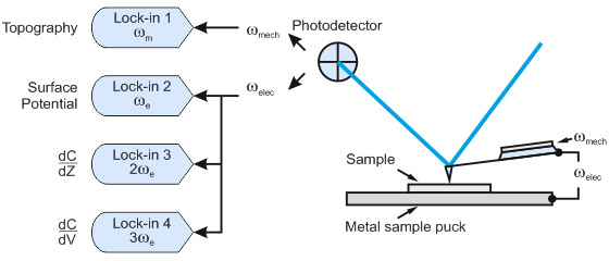
Fig. 1. A set-up for AFM-based electrostatic modes and possible configurations of lock-in amplifiers for multi-frequency electrostatic force studies
The AFM modes, which are based on the detection of tip-sample electrostatic forces [1], include Electrostatic force microscopy (EFM), Kelvin probe force microscopy (KPFM) and probing of local dielectric properties in various configurations including Maxwell stress microscopy and others [2], [3]. These modes were introduced for mapping the variations of electrostatic force, measurements of local surface potential and dielectric permittivity.
In these methods a conducting probe exercises the electrostatic force of a sample, which can be rationally modeled by considering a probe tip as an electrode in a tiny capacitor which it forms with the sample that acts as the second electrode, Figure 1 (right).
In these methods a conducting probe exercises the electrostatic force of a sample, which can be rationally modeled by considering a probe tip as an electrode in a tiny capacitor which it forms with the sample that acts as the second electrode, Figure 1 (right).
For the operation of AFM-related electrostatic modes the probe is driven into a mechanical oscillation by a piezo-shaker at its flexural mode, ωmech, and the electrostatic forces are stimulated by a DC electric bias applied to the probe and/or an AC bias either at ωmech or at other frequency, ωelec.
While scanning, the conducting probe simultaneously senses the mechanical and electrostatic force interactions with the sample.
The effects of these interactions can be decoupled either by performing these measurements in separate passes at the same frequency (two-pass technique) or in the single-pass with the simultaneous detection of the mechanical and electrostatic interactions at different frequencies [2]. The latter approach requires a use of several lock-in amplifiers in the detection system, Figure 1 (left).
The effects of these interactions can be decoupled either by performing these measurements in separate passes at the same frequency (two-pass technique) or in the single-pass with the simultaneous detection of the mechanical and electrostatic interactions at different frequencies [2]. The latter approach requires a use of several lock-in amplifiers in the detection system, Figure 1 (left).
References
- Y. Martin, D. A. Abraham, and H. K. Wickramasinghe “High-resolution capacitance measurement and potentiometry by force microscopy” Appl. Phys. Lett. 1988, 52, 1103–10005.
- S. Magonov, J. Alexander, and S. Wu “Advancing characterization of materials with Atomic Force Microscopy – based electric techniques”. In Scanning Probe Microscopy of Functional Materials: Nanoscale Imaging and Spectroscopy; Kalinin, S. V.; Gruverman, A., Eds.; Springer: Berlin, Germany, 2010; pp 233–300.
- H. Yokoyama, and M. J. Jeffery “Imaging high-frequency dielectric dispersion of surfaces and thin films by heterodyne force-detected scanning Maxwell stress microscopy” Colloids Surf. A 1994, 93, 359–373.