


Exploring Materials with AFM-based Electrostatic Modes
Application Note 084 (pdf 8.4 Mb)
- Electrostatic Force Microscopy: Experiments and quantitative analysis
- Local surface potential studies with single-pass Kelvin Probe Force Microscopy
- Broad range applications: From organic photovoltaics to metals and semiconductors
The applications of Atomic Force Microscopy are enriched by recent developments in the techniques based on the local probing of tip-sample electrostatic interactions. The range of materials that can be explored with such techniques is much broader than that for nanomechanical studies and includes not only soft organic and polymers compounds but also ceramics, metals and semiconductors. The individual components of complex materials can be distinguished due to differences of their surface potential, dielectric response and local conductivity. A whole suite of the AFM-based electrostatic methods, which includes Electrostatic Force Microscopy (EFM) and Kelvin Probe Force Microscopy in single- and double-pass implementations, is available in NEXT scanning probe microscope for quantitative studies of local electric properties. This application note presents the experimental EFM and KPFM studies performed on variety of samples.
FOREWORD
In the last twenty years characterization of structure and properties of materials at small length scales has been empowered by developments in Atomic Force Microscopy (AFM) [1] and related techniques. The use of a microscopic probe for high-resolution imaging of surface morphology and nanostructures has already been proven with the first AFM applications. Furthermore, the capabilities of this technique have been gradually expanded to the detection of local mechanical and electrical properties. The latter are successfully applied for distinguishing components in heterogeneous materials with high spatial resolution. Naturally, the probe sensitivity to different materials’ properties raises the question about its possible use for local quantitative measurements of these properties. There are a number of challenges along the way towards reliable quantitative analysis of specific mechanical and electrical properties that demands interplay between experimental and theoretical approaches.
In this Application Note we’ll demonstrate the capabilities of AFM methods based on the detection of tip-sample electrostatic interactions, which are realized in the NEXT Solver microscope. After a short description of these methods, which include the appropriate theoretical background, we will demonstrate the capabilities of the microscope by several practical examples obtained on different samples. They include self-assemblies of fluoroalkanes on various substrates, organic materials for electronics, polymers, metal alloys and semiconductor structures. The important issues of optimization of the experimental studies with AFM-based electrical modes and quantitative data analysis will be also discussed.
DETECTION OF ELECTROSTATIC TIP-SAMPLE INTERACTIONS
The AFM modes, which are based on the detection of tip-sample electrostatic forces [2], include Electrostatic force microscopy (EFM), Kelvin probe force microscopy (KPFM) and probing of local dielectric properties in various configurations including Maxwell stress microscopy and others [3, 4]. These modes were introduced for mapping the variations of electrostatic force, measurements of local surface potential and dielectric permittivity. In these methods a conducting probe exercises
the electrostatic
force of a sample, which can be rationally modeled by considering a probe tip as an electrode in a tiny capacitor which it forms with the sample that acts as the second electrode, Figure 1 (right). For the operation of AFM-related electrostatic modes the probe is driven into a mechanical oscillation by a piezo-shaker at its flexural mode, ωmech, and the electrostatic forces are stimulated by a DC electric bias applied to the probe and/or an AC bias either at ωmech or at other frequency,
ωelec. While scanning, the conducting probe simultaneously senses the mechanical and electrostatic force interactions with the sample.
The effects of these interactions can be decoupled either by performing these measurements in separate passes at the same frequency (two-pass technique) or in the single-pass with the simultaneous detection of the mechanical and electrostatic interactions at different frequencies [2].
The latter approach requires a use of several lock-in amplifiers in the detection system, Figure 1 (left). In this application note, we will describe these complimentary ways of characterization of local electric properties and then illustrate them with the practical examples on a standard sample – self-assemblies of semi-fluorinated alkanes F14H20[CF3(CF2)14(CH2)20CH3] on a Si substrate [5].
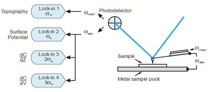
Figure 1. A set-up for AFM-based electrostatic modes and possible configurations of lock-in amplifiers for multi-frequency electrostatic force studies
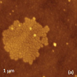
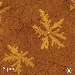
Structure of the F14H20 molecule and its dimensions are shown in Figure 2a. On substrates such as Si and mica the fluoroalkane molecules with fluorinated and hydrogenated parts self-organize into flattened domains with a fluorinated exterior. Morphology of a commonly observed self-assembly on Si is shown in Figure 2b. The overall molecular dipole of F14H20 is strong (3.1D) and oriented along the chain with the negative charge contribution in the fluorinated
part. The vertical orientation of the molecules, which is suggested for the flat self-assemblies on a number of substrates, leads to their strong surface potential.
The first mode of the AFM-based electrostatic force techniques for consideration is EFM.
In this two-pass technique, the probe detects surface profile in the first pass by measuring the mechanical tip-sample interactions at its flexural resonant frequency (1st Eigen mode) - ωmech. In the second pass, the probe follows the learned profile shifted 10-40 nm above the sample, and its response to the long-distant electrostatic force is detected.
The electrostatic tip-sample force is additionally stimulated by DC bias applied to the probe. Sensitive measurements can be realized either by recording the change of the phase and amplitude of the conducting probe, which is driven at ωmech, or by measuring the frequency and amplitude changes when the phase of the probe is kept constant. The relationship between the conservative electrostatic force and the probe phase (Ѳ) and amplitude (A) are described by following equations [6-7]:
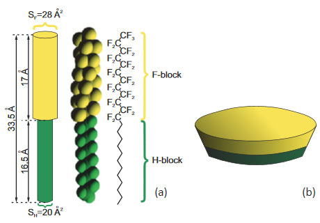
Figure 2. Molecular structure of F14H20 (a) and a model of the fluoroalkane self-assembly on Si substrate (b)
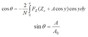
where A0 – the probe amplitude prior to its engagement into tip-sample force interactions; Zc – an averaged position of the cantilever over a surface during oscillations, and
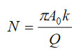
(k and Q – spring constant and quality factor of the probe at 1st flexural resonance). Alternatively, the frequency (ω) and amplitude changes, which are happening during the operation with the phase constant (near 90 degrees), are related to the electrostatic force by next expressions:
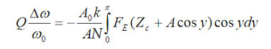
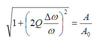
where ∆ω = ω - ω0 and ω0 - the frequency of the probe 1st flexural resonance (=ωmech). The equations (1) – (2) are instructive for determination of the electrostatic force from AFM measurements. The results can be further employed for extraction of the specific material properties once the appropriate relationship between the electrostatic force and a particular electric property is established. This approach is even more general because it can be applied for the analysis of probe-sample mechanical forces. The main complication, however, is the finding of the force-property relationship, which requires development of realistic models of the probe-sample interactions, most likely, with the help of the finite element analysis (FEA).
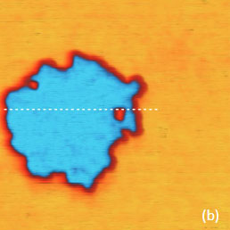
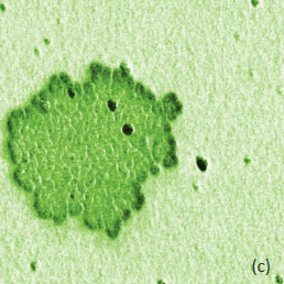
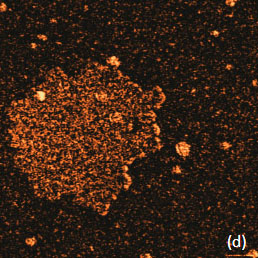
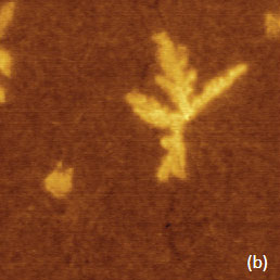
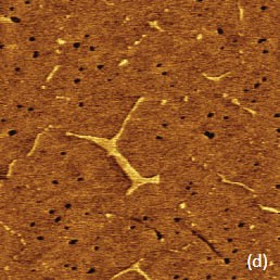
For the case of the electrostatic interactions several types of samples should be examined and analyzed with AFM-based electric modes. They include dielectric layers on a conducting substrate, samples with molecular dipoles, metals with different work functions, semiconductors with various doped regions, etc. The experimental examples collected in this application note can be considered as the first steps of the comprehensive analysis of local electric properties of various materials. The presentation of the experimental data we begin with the EFM images of F14H20 self-assemblies on Si wafer – the sample that has been already used as a standard specimen for verifications of different KFM operations [3], Figure 3a-f. The height image in Figure 3a shows several F14H20 domains, which are approximately 4 nm in height. These domains are composed of closely packed, spiral-like, nano-objects with almost vertically oriented molecules.
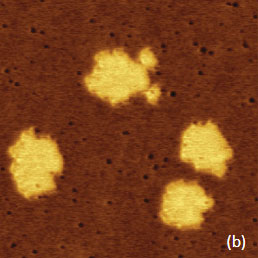
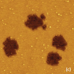
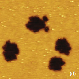
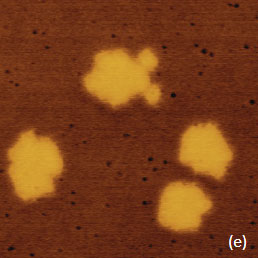
The phase and amplitude images correlate with each other in compliance with equation (1), and their contrast over the F14H20 self-assemblies reflects the strength of the attractive electrostatic interactions between the conducting probe and the vertically oriented molecular dipoles. The brighter phase and darker amplitude patches over the self-assemblies is consistent with the increase of the attractive force interactions over the self-assemblies. The strength of these interactions decreases with the probe-sample separation as evident from the weaker phase and amplitude contrast in the images recorded at an elevation of 30 nm (Figure 3e-f). The spatial resolution of the amplitude image is degraded as the probe further from the sample. The contrast of the frequency image, which was obtained while the phase was kept constant, also points on the stronger electrostatic force when the probe is positioned over the F14H20 domains in direct correlation with the equation (2). Although the amplitude, phase and frequency variations reflect the alternation of local electric properties and can be applied for compositional imaging, it is important to determine how to extract from these data the quantitative information such as strength and orientation of molecular dipoles in case of F14H20 self-assemblies. In the general case, the change of electric potential (D) at molecular dipoles can be expressed as:
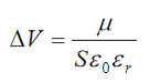
where μ - the molecular dipole moment, S - an area occupied by a single molecule; ε0 - universal dielectric constant, εr - relative dielectric permittivity.
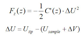
The electrostatic force, which acts vertically between the probe apex and a sample, can be presented as
We have applied a commercial FEA program from Field Precision Inc. to calculate the capacitance gradient for a particular probe-sample configuration and the results are summarized in Figure 4a-b. The electrostatic force dependence on the tip-sample separation is fit well by the following relationship with two parameters B1 and B2:
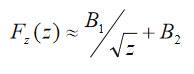
This finding allows a representation of the electrostatic force as 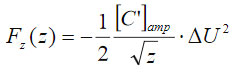 where the capacitance gradient
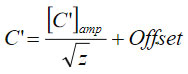
This substantially simplifies the integral
from the equation (1) that can be presented in analytical form. Finally, the solution of the problem can be reduced to the following equation
which contains the experimentally measured separation (Zc) and amplitude as well as the material properties: the capacitance gradient and the surface potential ∆V. The properties can be determined by solving this equation for a couple of measurements with different bias voltages (Utip). In our EFM measurements the tip bias is +3 V. A complete solution of the problem will be described elsewhere [9].
The described procedure is a rather complicated way to get the surface potential when it can be measured directly but this is not always the case. The measurements of the surface potential can be achieved in KPFM either in the double-pass or single-pass operation. In the 2nd pass of the double-pass operation the conductive probe is excited electrically at ωelec and the amplitude of the oscillation signals about a difference of surface potentials of the probe and a sample. A compensation
of the difference (i.e. nullification of the amplitude) by DC voltage applied to the sample (i.e. finding surface potential) is the function of KPFM servo.
Although the double-pass technique is broadly applied in the ambient studies, the remote position of the probe while recording the electrostatic force in the 2-pass limits sensitivity and spatial resolution compared to the probe placed in the immediate vicinity of a sample. The verification of this statement can be found in the comparison of the experimental data obtained in double- and single-pass operations described in our earlier application note [10].
In single-pass operation, which is enabled by the lock-in amplifiers, the probe responses at ωmech and much lower frequency ωelec define the separate of the mechanical and electrostatic forces. Besides the detection of the electrostatic force at the ωelec, one can record the force variations at 2ωelec and 3ωelec frequencies using additional lock-in amplifiers, Figure 1b. The variations of the force at 2ωelec can be used to obtain the image of
the capacitance gradient dC/dZ, which is related to the local dielectric response. The 3ωelec response is related to dC/dV [11].
A straight implementation of the single-pass KPFM operation is achieved by registration of the ωmech and ωelec (<< ωmech) responses with the lock-in amplifiers that collect the photodetector signal in parallel. In this case, the amplitude at ωelec (non-resonant frequency) is directly related to the electrostatic force and we define such imaging as AM-KPFM, where AM connotes for amplitude modulation. Its long-distant character results in an overall
force that combines contributions of the tip apex, tip body and the cantilever. To improve the KPFM sensitivity and spatial resolution one can use another approach, which we named PM-KPFM, where PM connotes for phase modulation [10]. In PM-KPFM, the electric excitation is made at low frequency that is within the bandwidth of ωmech (typically 10 kHz). Therefore, the photodetector signal contains the response at ωmech and its satellites at ωmech ± ωelec.
To make use of this resonance-like enhancement of the electric signal, the lock-in amplifiers are connected in-series. The 1st lock-in amplifier is managing the signal at ωmech that further is employed by the topography servo. The electric-related signal, which as can be chosen as cosѲ at ωelec is detected with the 2nd lock-in and it is used for KPFM servo. The dependence of the cosѲ on the force is defined by the integral I(Zc,A) that in the approximation
of small amplitudes is approximated by the force gradient similar to the approach described in [12]. It has been already shown that the use of force gradient can be rationalized as a confinement of the probe-sample interactions to the apex-sample junction therefore making them more sensitive and higher spatial resolution than those in AM-KPFM [13-14]. Again, the additional lock-in amplifiers in the case of PM-KPFM can be used for recording the 2ωelec and 3ωelec responses. In an alternative
approach, the contributions of the tip’s body and cantilever to the total electrostatic force can be reduced with a use of special probes that have an extremely long tip (~100 micron). The images in Figure 5a-f illustrate the KPFM measurements on the F14H20 self-assembly on Si. A comparison of the height, surface potential and amplitudes in the 2ωelec and 3ωelec images shows a couple of important features.
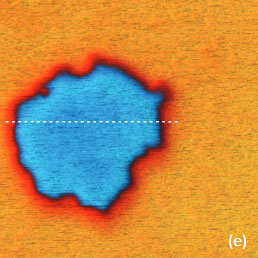
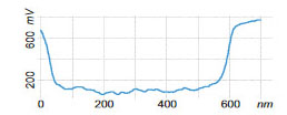
Surface Potential, AM
The surface potential recorded in the PM-KPFM mode is larger than one obtained in the AM-KPFM mode. Several particles around the F14H20 domain distinguished in the height image are not present in the surface potential image but are seen in the amplitude images. Most likely, these particles do not have molecular dipoles or at least ones that are oriented vertically. The same particles being between the tip and the sample influence the capacitance of this junction, which
is manifested in
the amplitude images. The changes of the 2ωelec signal are related to dielectric permittivity (εr) of the adsorbate layer and its thickness (h) being a function of their ratio h/εr. As we have already shown the dielectric permittivity can be extracted from the 2ωelec data for thin films of polystyrene - PS and poly(vinyl acetate) – PVAC [7].
The measurements of dC/dV response were earlier applied for studies of semiconductors and should be further expanded to different materials. Particularly, the dC/dV images on a Si test sample demonstrated contrast dependence on the species and density of dopants [11].
SELECTED EXAMPLES OF EFM AND KPFM
In following we will consider several examples of EFM and KPFM studies of different materials. In many instances, successful imaging was achieved either in KPFM or EFM mode. Furthermore, the quality of the surface potential image is not always superior in PM-KPFM mode as compared to AM-KPFM. A choice of probe is also important for improving either sensitivity of electrostatic force detection or spatial resolution of the imaging. Therefore, practical experience in studies of different materials can be very helpful for the optimization of AFM-based electric studies.
Self-assemblies of F14H20 fluoroalkanes on different substrates
KPFM studies have been applied for exploring the molecular order of fluoroalkanes on different substrates [3], and the images of their self-assemblies on mica and MoS2 are presented together with several cross-section profiles in Figure 6a-f.
Surface Potential, PM
Surface Potential, PM
In the case of F14H20 adsorbates on mica, the fluoroalkanes form domains, which consist of spirals and ribbons, and which resemble those observed on a Si substrate. The height of one of such domains is close to 4 nm, and the surface potential difference with mica is around 1V (Figure 6b, c) and higher [3].
With another layered material that has atomically smooth surface, MoS2, we observed the lamellar patches, whose thickness is close to a diameter of individual fluoroalkane molecule (~0.3 nm), and thicker islands with 1 nm in height, Figure 6d. A part of the patch, with a lamellar spacing of 6.2 nm, is magnified in the insert of this image. Such epitaxial order is similar to what is typically found on graphite, despite the fact that the lattices of these layered materials are quite different. Within the lamellae the individual fluoroalkanes molecules are lying parallel to the substrate and, therefore, the surface potential of this patch is only 100 mV.
The 1-nm thick island exhibits a contrast of ~250 mV higher than its surrounding. This is quite unexpectedly because we have not previously observed the F14H20 contrast brighter than substrate’s potential contrast for F14H20 adsorbates on Si, mica or graphite. We suggest that the average orientation of the molecular dipoles is slightly towards MoS2, and further experiments are needed to support this hypothesis.
Organic materials for electronics and solar cells
With the increasing use of organic materials for field effect transistors and solar cells, the characterization of their electric properties becomes very important. We will consider the following examples for imaging - pentacene, oligothiophene layers and surface of P3HT (poly-3-hexylthiophene) blended with the fullerene derivative [6,6]-phenyl-C61 butyric acid methyl ester (PCBM) on ITO glass. Organic semiconductors, most notably pentacene, have attracted attention as channel materials in thin film transistors because these devices have a field-effect mobility of around 1 cm2V-1sec-1 and a current modulation of 107-108.
The exceptional performance of pentacene films in field effect transistors is due to the favorable crystal packing in the polycrystalline film morphology with molecules oriented almost perpendicular to the substrate, yielding a high degree of intermolecular p–orbital overlap in the film plane. In the transistor setting the gate-induced charge is electrostatically confined to the organic-isolator interface; structure and electric properties of the first few monolayers of pentacene
immediately adjacent to the dielectric surface are crucial for transistor performance.
We examined a sample of vapor-deposited pentacene on a Si substrate. The height image showed a single layer on Si with individual grains separated by dark border lines as well as few dendritic structures of the second layer. The EFM and KPFM images collected from the same location are presented in Figure 7b-d.
Remarkably, the amplitude and frequency images obtained in double-pass EFM and the surface potential image obtained in single-pass PM-KPFM mode revealed contrast differences only between parts of the dendritic structures and the first layer. Earlier, these samples were examined with the so-called transverse shear microscopy (TSM) mode [15] that senses the difference of AFM probe lateral interactions along various crystallographic directions in the pentacene grains of the 1st molecular layer on Si substrate. Also the branches of the dendritic structures exhibit the different TSM contrast depending on their epitaxy type to the underlying pentacene domains.
The correlation between the surface potential and epitaxial nature of the grains was previously documented [16]. These contrast differences have been tentatively assigned to variations of the electrostatic coupling between the induced dipoles at the interfaces between the pentacene layers and its interface with the substrate.
The effects seen in the Figure 7b-d seems to be in line with earlier observations [16], and we can explain the contrast of the dendritic structures in EFM and KPFM images by dissimilar electrostatic interactions of their parts, which are spread over different grains of the 1st layer. In any case, the characterization of the local electric properties of organic layers is very helpful in controlling and monitoring the performance of these layers in transistor devices. This statement
is further confirmed by EFM studies of the films of oligothiophene (OTh) films on Si, which are used for field effect transistors.
The OTh samples we have examined were prepared by spin-casting from a toluene solution on Si substrate. The molecules contain 7 thiophene rings, which are prepared with linear aliphatic chains as the end groups to make the material soluble in organic solvents [17]. In the solid state, OTh molecules behave similar to pentacene molecules and tend to pack with their long axis parallel to each other, forming stacks of layers with a thickness defined solely by the molecular length.
The observed structural anisotropy favors charge transport in the direction parallel to the layers. This material has already been tested in the ultrathin layer organic transistor and the surface potential profile across the layer was monitored for performance evaluation [18]. The EFM images of the OTh samples with different coverage on the Si substrate are presented in Figure 8a-f. In this case, double-pass EFM images have shown much more reproducible and strong contrast compared to KPFM. In
the sample with sub-monolayer OTh coverage the height image reveals near rectangular domains, some of which are merged into larger flat aggregates.
The dark phase contrast of these domains points to an increase of the electrostatic tip-sample interactions compared to the substrate. With monolayer coverage (Figure 8c) the height image shows an almost complete 1st layer with border lines between the grains. There are a number of small droplets and fibers of the material on top of the surface of the 1st layer, and they exhibit darker phase contrast when compared to the underlying layer and the substrate, Figure
8d.
This reveals a possible heterogeneity of local electric properties that is not desirable for ultrathin layer transistors. Furthermore, with the increase of coverage, the multi-layer morphology is formed by island nucleation and the three-dimensional crystal structures continue growing by the screw dislocation mechanism, Figure 8e. The related phase image in Figure 8f shows that the contrast of the top layers becomes more negative, which further complicates the electrostatic field on such samples. Therefore, the EFM and KPFM studies of organic ultrathin films of pentacene and oligothiophenes proposed for organic transistors can provide useful information regarding the films microstruc ture, electric properties and performance during device operation.
In recent years substantial progress has been made in the development of the organic solar cells. We will illustrate the application of the AFM-based electric modes in examining photovoltaic materials by examples of EFM and KPFM imaging of a P3HT/PCBM blend. P3HT/PCBM has reported an efficiency as high as 5%, which is unusual in organic photocell material. PCBM is a fullerene derivative.
Because of the high electron-hole mobility, it plays the role of electron acceptor in many organic cells. It is the excitation of the π-orbital electron in P3HT that gives the photovoltaic effect in the blend. P3HT performs as a conducting polymer due to crystallization and chain stacking of the thiophene moieties. The sample of P3HT/PCBM was prepared as a thin film by spin-casting of its solution in toluene on a conducting ITO glass substrate. The height image of this sample shows a slightly corrugated morphology with distinctive nano-fibrillar features of 20-30 nm in width, Figure 9a. Such features are common to P3HT polymers and have been observed in TEM [19] and AFM [20] micrographs of this material. These results also suggest that the film formation process is accomplished with a predominant aggregation of the P3HT polymer in the surface layer.
The phase and amplitude images obtained in EFM exhibit the contrast variations associated with the nanofibrils and the phase contrast is most pronounced, Figure 9b-c. A comparison of the height and phase images shows that the nanofibrils’ body has a darker phase contrast than the interfibrilar spacing, which is related to the enhancement of the electrostatic tip-sample interactions. This effect can be attributed to molecular dipoles because the surface potential images exhibit similar features with surface potential variations across the nanofibrils being in the 0-80 mV range, Figure 9d. We can tentatively attribute these effects to the interfacial dipole moments induced by the molecular orientation and electronic coupling in the materials [21].
Polymers: Thermoplastic vulcanizate and thin film of PS-PVAC blend
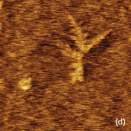
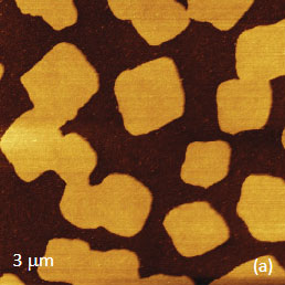
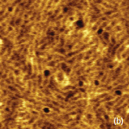
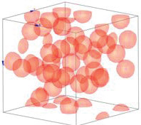
AFM studies of polymer materials have been performed for over twenty years by researchers in academia and industry. Although the compositional mapping of such materials is usually achieved based on the differences of the mechanical properties of the constituents, variations of the local electric properties can be also employed for this purpose as well. We will illustrate this on a couple of examples. Studies of carbon black filled plastic and rubber compounds are of high technological importance due to their broad range of applications. The examination of structure-property relationships and factors that contribute to tuning their particular properties requires comprehensive microscopic analysis with AFM being one of the appropriate techniques. A composite sample of thermoplastic vulcanizate (TPV) made of a blend of isotactic polypropylene and EPDM rubber filled by carbon black particles and several other materials was examined. A sketch of the distribution of carbon black particles is presented in Figure 10. Structure of TPV is characterized by the microphase-separated morphology of the rubbery and plastic components and by the dispersion of carbon black particles (20‑40 nm in diameter) forming a conducting percolation network.
The use of EFM for observations of the percolation network of the carbon black filled material has previously been demonstrated in 1995 [22].
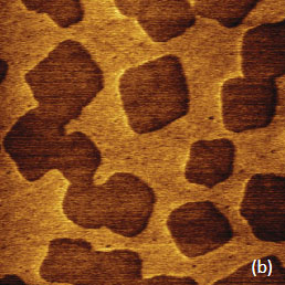
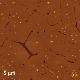
We have examined the surface of a TPV sample, which was prepared by hot melting between two flat substrates, with KPFM and EFM modes. The EFM images show the most pronounced contrast whereas the dC/dZ response was weaker and the surface potential image exhibit only faint features because the PP/EPDM blend is good dielectric and does not contribute to the response. The height image of the sample shows surface corrugations and a number of small particles, Figure 11a. The EFM amplitude and phase images are characterized by multiple locations with sharp contrast compared to the almost features-less surrounding. These locations can be assigned to the electrostatic force variations caused by the electrostatic interactions of the probe with the carbon black particles contributing to the percolation network. The magnified view showing a correspondence between the particles seen in the height image and in the amplitude image is given in Figure 11d-e.
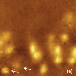
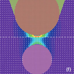
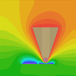
Two bright spots are indicated with white arrows in the low left corner of the amplitude image, Figure 11e. The bright spots corresponds to a particle seen on the sample surface in Figure 11d, the weaker spot does not have a similar partner in the height image. Most likely, the weaker intensity spot reflects the interaction of the probe with a sub-surface carbon particle. To justify this assignment, We have conducted FEA simulations of the electrostatic force between a conducting AFM probe and a small conducting particle immersed in a dielectric matrix, Figure 11f. Indeed, the color-coded force profiles of the probe-sample electrostatic force demonstrate the sensitivity of the probe to sub-surface particles.
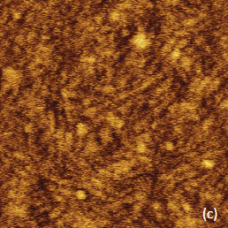
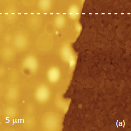
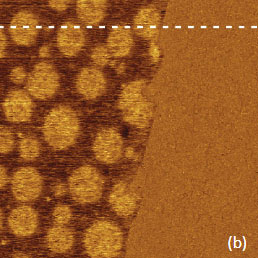
Another example of local electric studies of polymers is taken from the examination of a thin film of a PS/PVAC blend deposited on an ITO substrate. The compositional imaging of a similar sample was performed with the confocal Raman/AFM instrument (NTEGRA Spectra, NT-MDT SI) by mapping of polymer-specific scattering bands this allows assignment of the matrix to PS and the round-shaped domains to PVAC. We also conducted dC/dZ measurements of the films of PS/PVAC and its individual components and demonstrated a path towards local quantitative measurements of their dielectric permittivity [7]. Here we are presenting the KPFM images obtained on the PS/PVAC film on an ITO substrate, Figure 12a-f.
Surface Potential, PM
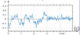
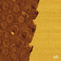
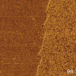
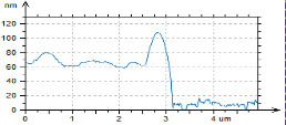
These measurements were performed near a scratch, which was made with a sharp wooden stick. This scratch removed only the polymer overlay without damage to the underlying substrate, in order to facilitate the measurement of the film thickness and to get the contrast difference between the substrate and the blend components. The height image in Figure 12a shows the film edge, and the microphase separation morphology is seen on the left. A surface pattern common to the conducting ITO glass is observed on the right. The profile across the edge indicates that the film thickness is around 70 nm. The surface potential contrast is different between the substrate and the blend components with the highest contrast from the circular domains of PVAC, which are embedded into the PS matrix, Figure 12b. The fact that the PVAC domains have ~200 mV higher potential than the PS matrix can be explained by the stronger dipole moment of PVAC and its orientation towards the substrate.
The contrast in the amplitude (2ωelec) image (Figure 12d) reflects a dielectric permittivity (εr) of the blend film and local variations related to the h/εr ratio, where h – film thickness. The approach to extract the dielectric permittivity from such data was documented elsewhere [7]. The contrast of the amplitude (3ωelec), Figure 12e, is less specific yet it differentiates the substrate and polymer film.
Metals and semiconductors
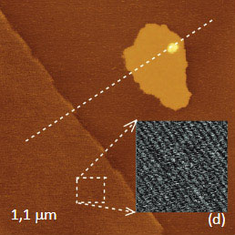
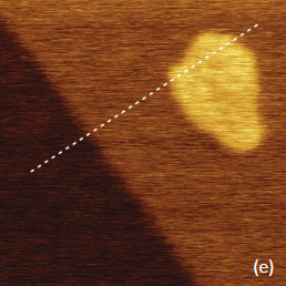
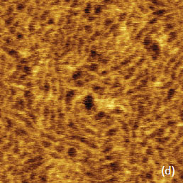
The use of AFM-based electric modes enables the characterization of heterogeneous rigid materials such as metals and semiconductors. The individual components of these materials could not be distinguished with AFM nanomechanical modes because the probes are usually much softer than the objects of interest. However, variations of the metal work function can be detected with KPFM as we have demonstrated by imaging two incomplete metal alloys of bismuth (Bi) and lead (Pb) with tin (Sn), which are used as common soldering materials.
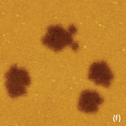
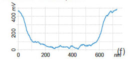
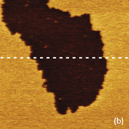
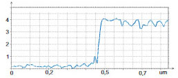
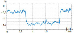
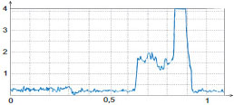
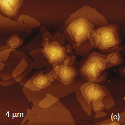
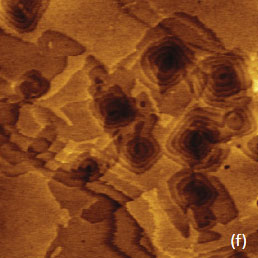
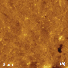
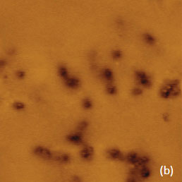
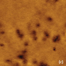
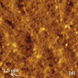
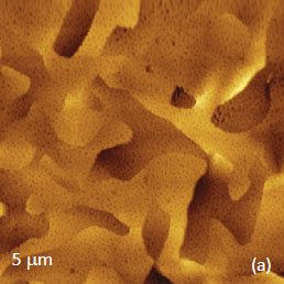
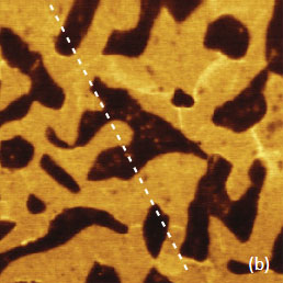
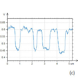
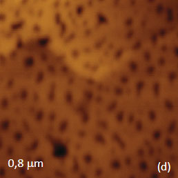
The samples of the alloys were prepared by hot melting of small pieces at 190 °C between flat substrates like mica or Si. After cooling of the specimens to room temperature, the substrates were easily detached from the alloys whose glanced metal surfaces were examined in AFM studies. The height and surface potential images of the metallic alloy Bi/Sn are shown in Figure 13a-f. The contrast of the surface potential image is practically binary with difference over 150 mV (Figure 13c). The surface topography of hot-melted BiSn sample is characterized by variety of small domains with dimensions of few microns, Figure 13a.
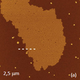
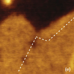
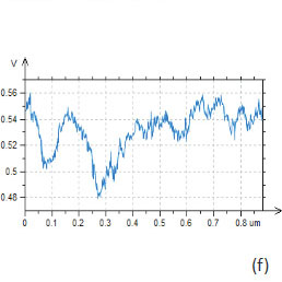
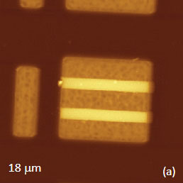
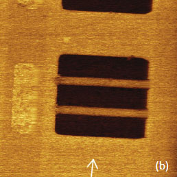
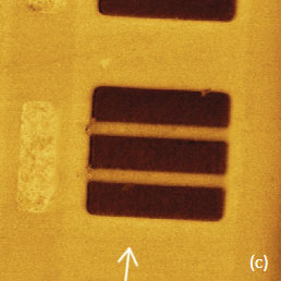
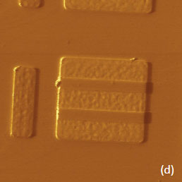
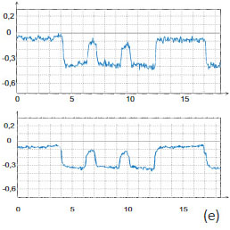
The contrast of the surface potential image is practically binary with difference over 150 mV (Figure 13c). As it was mentioned in [3], the potential contrast can be assign to differences of the work function of Bi (4.22V), Pb (4.25V) and Sn (4.42V) [23]. The work function is an essential characteristic of metals, which defines their important properties such as electron emission, corrosion, photosensitivity, and surface potential. Keeping in mind that in the measurements we have used a Pt-coated probe (work function of Pt – 5.65 V), therefore the lower surface potential areas in the images of the alloys can be assigned to Sn domains. When such measurements are performed at ambient conditions, one should be aware of the tip and sample variations and possible influence of contaminations. These factors have definitely influenced our KPFM studies performed in air. The crucial question about the possible use of surface potential for quantitative analysis of doping density is still open. Doping profiles can be deduced from KPFM measurements to the extent that variations of work function and capacitance are related to the dopant type and concentration at or near the sample surface [24, 25]. Surface potential studies of the SDRAM structures are presented in Figure 14, 15. In the studies of large-scale structures with regular shapes as one shown in the height image (Figure 14a) the use of closed loop operation is essential.
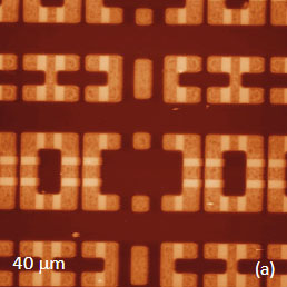
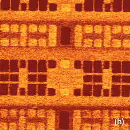
A comparison of the height and surface potential image recorded in AM-KPFM mode reveals the potential map and it is different from topography because reflects the doped regions.
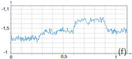
The use of AM-KPFM in imaging of large-scale structures with sharp corrugations is preferable to the PM-KPFM mode because the latter, which is based on the detection of force gradient, gives more noisy surface potential signal at the steep edges of topographical profiles. This is confirmed in the images shown in Figure 15a-e. The surface potential profile obtained in AM-KPFM mode is less noisy than the similar profile extracted from the PM-KPFM image, Figure 15e. It is worth noting that using conducting probes with a larger tip radius is favorable for further improvement of the signal-to-noise performance of the electric mode when spatial resolution can be slightly sacrificed.
CONCLUSIONS
We have described a very comprehensive suite of AFM modes, which is based on the detection of the probe-sample electrostatic forces and is realized in NEXT scanning probe microscope. The set includes single-pass and double-pass EFM and KPFM as well as measurements of capacitance gradients. The overall and challenging goal of these methods is the quantitative characterization of local electric properties, which can be outlined as a sequence of several steps. The first step is recording reliable and accurate probe responses (a change of frequency, amplitude or phase of the conducting probes or a direct measurement of surface potential) uniquely related to the tip-sample electrostatic interactions. Only in case of KPFM we directly record the specific material property i.e. surface potential.
The obtained experimental information can be sufficient for compositional mapping of heterogeneous materials if the images exhibit satisfactory contrast related to the individual components.
The more challenging task is the extraction of quantitative information from EFM and dC/dZ data. This goal can be accomplished through the theoretical analysis of the data that involves a conversion of the probe’s responses to variations of electrostatic force and determining the appropriate force-property relationship. In the earlier application note and paper [7] we have shown a method of calculating the quantitative dielectric permittivity from the dC/dz data. In this application note the analysis of the EFM images in terms of local surface potential and strength of the molecular dipoles was demonstrated. This analysis has been substantially facilitated by use of FEA, which provides a more realistic description of the probe-sample electrostatic interactions in the AFM-related geometry. Therefore, the developed theoretical approaches fully support the experimental data obtained with NEXT scanning probe microscope on the way to comprehensive characterization of local electrical properties of materials.
ACKNOWLEDGEMENTS
We are thankful to the researchers: Prof. M. Moeller and Dr. A. Mourran (DWI, Aachen, Germany), Dr. G. Haugstad (University of Minnesota, USA), Prof. M. Irwin (University of Texas, El Paso, TX) who kindly provided us with the samples used for the imaging described in this application note.
REFERENCES
1. G. Binnig, C. F. Quate, and Ch. Gerber “Atomic force microscope” Phys. Rev. Lett. 1986, 56, 930–933.
2. Y. Martin, D. A. Abraham, and H. K. Wickra-masinghe “High-resolution capacitance measurement and potentiometry by force microscopy” Appl. Phys. Lett. 1988, 52, 1103–1105.
3. S. Magonov, J. Alexander, and S. Wu “Advancing characterization of materials with Atomic Force Microscopy – based electric techniques”. In Scanning Probe Microscopy of Functional Materials: Nanoscale Imaging and Spectroscopy; Kalinin, S. V.; Gruverman, A., Eds.; Springer: Berlin, Germany, 2010; pp 233–300.
4. H. Yokoyama, and M. J. Jeffery “Imaging high-frequency dielectric dispersion of surfaces and thin films by heterodyne force-detected scanning Maxwell stress microscopy” Colloids Surf. A 1994, 93, 359–373.
5. A. Mourran, A.; Tartsch, B.; Gallyamov, M.; Magonov, S.; Lambreva, D.; Ostrovskii, B. I.; Dolbnya, I. P.; de Jeu, W. H.; M. Moeller, “Self-assembly of the perfluoroalkyl-alkane F14H20 in ultrathin films”. Langmuir 2005, 21, 2308–2316.
6. S. Belikov, and S. Magonov “Classification of Dynamic Atomic Force Microscopy Control Modes Based on Asymptotic Nonlinear Mechanics” Proceedings American Control Society, St. Louis, 979-985, 2009.
7. S. Belikov, J. Alexander, I. Yermolenko, S. Magonov “Atomic Force Microscopy Control System for Electrostatic Measurements based on Mechanical and Electrical Modulation” Amer. Control Conference 2012, 3228-3233.
8. J. Alexander, S. Magonov, and M. Moeller “Topography and surface potential in Kelvin force microscopy of perfluoroalkyl alkanes self-assemblies” J. Vac. Sci. Technol. B 2009, 27, 903–911.
9. S. Belikov, J. Alexander, C. Wall and S. Magonov, “Tip-Sample Forces in Atomic Force Microscopy: Interplay between Theory and Experiment”. MRS Online Proceedings Library, Volume 1527, 2013, mrsf12-1527-uu02-04. doi.org/10.1557/opl.2013.616
10. Application Note “Single-Pass Measurements in Atomic Force Microscopy: Kelvin Force Microscopy and Local Dielectric Studies”, Application Note 082, NT-MDT Spectrum Instruments . It can be downloaded from https://www.ntmdt-si.com/resources/applications.
11. K. Kobayashi, H. Yamada, K. Matsushige “Dopant profiling on semiconducting sample by scanning capacitance force microscopy” Appl. Phys. Lett. 2002, 81, 2629.
12. F. Giessibl “Forces and frequency shifts in atomic-resolution dynamic-force microscopy” Phys. Rev. B 1997, 56, 16010-16015.
13. U. Zerweck, CH. Loppacher, T. Otto, S. Grafstroem, and L. M. Eng “Accuracy and resolution limits of Kelvin probe force microscopy” Phys. Rev. B 2005, 71, 125424.
14. F. Krok, K. Sajewicz, J. Konior, M. Goryl, P. Piatkowski, and M. Szymonski “Lateral resolution and potential sensitivity in Kelvin probe force microscopy: Towards understanding of the sub-nanometer resolution” Phys. Rev. B 2008, 77, 235427–235429.
15. K. Puntambekar, J. Dong, G. Haugstad, and C. D. Frisbie “Structural and electrostatic complexity at a pentacene/insulator interface” Adv. Funct. Mater. 2006, 16, 879-884.
16. V. Kalihari, D. J. Ellison, G. Haugstad, and C. B. Frisbie “Observation of unusual homoepitaxy in ultrathin layers of pentacene films and correlation with surface electrostatic potential” Adv. Mater. 2009, 21, 1-7.
17. Matthieu Defaux, Fatemeh Gholamrezaie, Jingbo Wang, Andreas Kreyes, Ulrich Ziener, Denis V. Anokhin, Dimitri A. Ivanov, Armin Moser, Alfred Neuhold , Ingo Salzmann, Roland Resel, Dago M. de Leeuw, Stefan C. J. Meskers, Martin Moeller, and Ahmed Mourran “Solution-Processable Septithiophene Monolayer Transistor” Adv. Mater. 2012, 24, 973-978.
18. S. G. J. Mathijssen, E. C. P. Smits, P. A. van Hal, H. J. Wondergem, S. A. Ponomarenko, A. Moser, R. Resel, P. A. Bobbert, M. Kemerink,
R. A. J. Janssen & D. M. de Leeuw ”Monolayer Coverage and Channel Length Set the Mobility in Self-Assembled Monolayer Field-Effect Transistors” Nature Nanotechnology 2009, 4, 674-680.
19. S. Hugger, R. Thomann, T. Heinzel and T. Thurn-Albrecht “Semicrystalline morphology in thin films of poly(3-hexylthiophene)” Colloid Polym. Sci. 2004, 282, 932–938.
20. P. Vanlaeke, A. Swinnen, I. Haeldermans, G. Vanhoyland, T. Aernouts, D. Cheyns, C. Deibel, J. D’Haen, P. Heremans, J. Poortmans, and J.V. Manca “P3HT/PCBM bulk heterojunction solar cells: Relation between morphology and electro-optical characteristics” Solar Energy Materials Solar Cells 2006, 90, 2150-2158.
21. A. Tada, Y. Geng, Q. Wei, K. Hashimoto, and K. Tajima “Tailoring organic heterojunction interfaces in bilayer polymer photovoltaic devices” Nature Materials 2011, 10, 450-455.
22. R. Viswanathan, and M. B. Heaney “Direct imaging of the percolation network in a three-dimensional disordered conductor–insulator composite” Phys. Rev. Lett. 1995, 75, 4433–4436.
23. H. B. Michaelson “The work function of the elements and its periodicity” J. Appl. Phys.1977, 48, 4729–4733.
24. A. K. Henning, T. Hochwitz, J. Slinkman, J. Never, S. Hoffmann, Ph. Kaszuba, and C. Daghlian “Two-dimensional surface dopant profiling in silicon using scanning Kelvin probe microscopy” J. Appl. Phys. 1995, 77, 1888–1896.
25. T. Matsukawa, S. Kanemaru, M. Masahara, M. Nagao, H. Tanoue, and J. Itoh “Doping diagnosis by evaluation of the surface Fermi level using scanning Maxwell-stress microscopy” Appl. Phys. Lett. 2003, 82, 2166–2168.